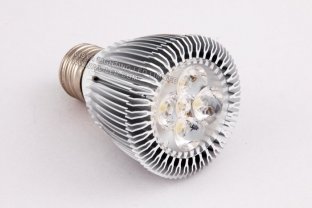
residential led light bulbs and MH lights design

Metal halide lamp is a third generation of electric light, because of its high luminous efficiency, long life such as led lights, play an increasingly important role in the green lighting. As an energy-saving lighting appliances, electronic ballasts, has become one of the key elements of the implementation of green lighting. Compared with the traditional magnetic ballast, electronic ballast volume and weight are greatly reduced, to improve network power quality, improved lighting quality. However, the universal application on the market today is the inductance ballast, mainly due to the simple structure, high reliability, and inexpensive. Therefore, the development of metal halide electronic ballasts higher requirements must be met to reliably start metal halide lamp; provide constant rated power; the need to eliminate the acoustic resonance phenomenon; protection function. In this paper, design for indoor lighting, small power metal halide lamp electronic ballast topology, to study the control strategy.

residential led light bulbs and MH lights design

Start-up phase and steady-state phases using the half-bridge parallel load resonant (ParallEL Load Resonant, referred to as PLR) circuit and the half bridge dual Buck circuit. Before the start of the metal halide lamp, the arc tube filled with inert gas is not ionizing, light in a high impedance state can be approximately considered to be open. In the startup phase in Figure 1 Relay disconnect switch VQ1 and VQ2 complementary high-frequency drive signal. Figure 2 shows the PLR ​​circuit. Parallel resonant capacitor Cp to generate high voltage and resonant inductor L (L1 and L2) in the high-frequency AC voltage, driven by resonance of the Cp at both ends.

From high frequency to low frequency, fc the closer fz, the greater the amplitude of Cp on the resonant voltage ur. The input voltage of the PLR ​​circuit is rich in odd harmonics of the square wave voltage. Fz, the fundamental frequency of the square wave voltage is higher than the circuit is designed only to consider the fundamental and ignore the impact of high harmonics; fz, if the fundamental frequency of square wave voltage is lower than the circuit must be considered high harmonic frequency, harmonic resonance may become a major part of ur. This article 3 times ur resonance, effectively reduces the series inductance in the startup current, improve the reliability of the power circuit.

Furthermore, using the right side of the resonant peak from high to low slip frequency, the resonant circuit can be realized in the emotional area, VQ1 VQ2 the zero-voltage, reducing MOSFET switching losses. Due to the discrete nature of the parameters, the design of the resonant peak (Figure 3, curve 2) may be to the left (Figure 3, curve 3) or right (Figure 3, curve 1) offset. If you rely on to set slip frequency cut-off point to control the boot process, when the resonant peak is shifted to the left, to the slip frequency cut-off point, ur may still be unable to lamp is lit; when the resonant peak is shifted to the right, the boot process may be slippery over the resonant peak, resulting in excessive ur damage to the power switch. Therefore, by setting start voltage ug limit amplitude control the slip frequency cut-off point. When the slip frequency of the high-pressure reaches the voltage limit amplitude, high pressure, automatic stop sliding frequency.

After the lamp is lit, the light from high-impedance characteristics into the nature of the low resistance. Until the lamp arc stability, lamp power reaches the set value, in Figure 1 Relay is closed, the drive signal into a low frequency square wave signal with frequency modulation. In this case, the circuit structure and operating mode has the obvious symmetry, Buck circuit characteristics in the low-frequency switching cycle, Figure 4 shows the structure of the half bridge dual Buck circuit. Lamp voltage u0 and lamp current io are low frequency square wave signal, can effectively inhibit the light acoustic resonance phenomenon. Because the square wave uo and io resistive when the volt-ampere characteristics of low power metal halide lamp, alternating positive and negative changes in lamp power AC component, which can not stimulate the resonator.


Design of electronic ballasts FREESCALE 8-bit microcontroller for the control of the core, the lamp power closed-loop control and protection functions by detecting the lamp terminal voltage uc and dc bus current, open circuit, short circuit and abnormal state when the light side ballast automatic protection. Figure 5 shows the control block diagram. Starts, the high-frequency square-wave signal control circuits output complementary control VQ1 off VQ2 the frequency from high to low slide, uc gradually increased, the limit set uc to control the slip frequency cut-off point. When when the uc suddenly landed, and to judge the value below the set, the ionized gas in the lamp arc tube, into a single frequency transient transition; when the lamp power reaches the set value, description of the lamp has been lit, to meet the switching conditions; Relay closed circuit from parallel load resonant switch to the half bridge dual Buck circuit structure, the control circuit output with high-frequency modulation of low frequency square wave signal, and the closed-loop control of steady state power. Half Bridge Dual Buck inputs of the circuit is of 400V Ubus, sampling will be able to link current approximate control lamp power. During the transition or steady state control stage light side open or short, you can automatically block the power circuit output, enter the state of the delay protection.

residential led light fixtures and car ballast

20 actual 80 years, the exact size of the small low-power quartz metal halide lamp to get a breakthrough in both design and production. Meanwhile, with people’s lives and exchanges between the quickening pace of completion of the highway, requires continuous improvement of the car at night driving safety, which requires headlamps visual construct, so the world began with a small power xenon metal halide lamps instead of the light of conventional halogen headlamp. Several atmospheric high-pressure xenon filled lamp(led lights) as a startup gas to meet the instantaneous luminous requirements of the automobile headlamp. At present, high-intensity car headlights electronic ballast system is one of the focus, but the electronic ballast design complexity, expensive and bulky, is only applicable to high-end cars and other applications. Obviously, if we reduce the size and cost, its demand will substantially increase, and therefore has a very good application prospects.

In this paper, analog control, auto headlamps electronic ballasts, the analog circuit to control the car headlights from the start to the stability control tasks, including constant power, ignition control.


(2) the basic circuit structure

In order to meet the different requirements of the lights in the startup and steady state, generally used in car headlights with electronic ballast circuit structure contains some of the features .

(1) DC / DC boost circuit due to the current automotive power for 12V lead acid batteries, lamp steady-state voltage of about 85V, and therefore must go through a step-up circuit battery voltage increased.

(2) high-voltage start circuit need high-voltage pulse to the lamp breakdown discharge and therefore require high-voltage start circuit lamp is lit. The start circuit can be taken one or two step-up manner to generate more high-voltage pulse of at least 23kV.

(3) DC / AC conversion circuit DC boost circuit output to DC, you must use the inverter circuit, DC into AC square wave current of the lamp required. The inverter circuit is generally a full-bridge inverter. The full-bridge inverter circuit to provide low-frequency AC square wave current to the lamp, in order to avoid the occurrence of acoustic resonance.

(4) when the lamp start of the drive and protection circuit to control start-up circuit. The lamp is lit, the detection voltage and short circuit occurred. Through the detection of lamp voltage and lamp current signal to control drive and protection circuits, lamp work stably.


residential led light fixtures and car ballast

Boost converter to meet the normal work requirements in light, we must also consider the no-load output voltage capability of the circuit. The no-load output voltage is decided by the circuit design of ignior circuit and take over.

(1) in the circuit topology, Boost circuit is the simplest. When the switch S in a large duty cycle, you can get a high output voltage. However, in this kind of work conditions, the output diode existence of the reverse recovery problem, the switch voltage and current stress, loss.

(2) For a forward converter, although it can achieve the purpose of the boost, but its no-load output voltage capability than the flyback converter. A forward converter transformer does not need to store energy, so the size of the transformer core can be very small, but must increase the number of turns of the secondary winding to the output voltage of 400V, and therefore require a large window area. Excessive secondary winding will lead to the increase of transformer copper loss and improve efficiency.

(3) Flyback converter as a DC / DC level topology by additional ignition winding, reducing the switch stress of the DC / DC level, increasing the reliability of the circuit; if the digital control circuit can work at the critical continuous state can achieve more, thereby reducing the circuit cost.


In addition, the main circuit topology of the car headlights electronic ballast comprehensive consideration of these methods is generally used as shown in Figure 2 Flyback converter and low-frequency full-bridge inverter circuit as the main circuit topology.

residential led lighting fixtures and smaller driver

As technology advances, LEDs are becoming smaller, lighter and higher efficacy. Order to allow the LED to produce the desired brightness, constant current LED driver circuit. Most of today’s cellular phones, miniature white LED and a small LED drive, full color LCD display, accurate and uniform brightness. The battery life is determined mainly by the brightness of the LCD when the phone is in call state, the LCD power consumption is about 1/3 of the total power budget. The LED itself and adjust the current driver circuit consumes power. Miniature LED driver applications, in addition to battery life, board space is also an important consideration, which makes the choice of the LED driver topology becomes more important than ever.

residential led lighting fixtures and smaller driver

LED driver topology: spatial factors

The most popular handheld devices battery is a lithium-ion battery, the battery voltage range of 4.2V when fully charged down to the discharge state is about 3.3V. In backlighting applications, the white LED panel current of 20mA typically demonstrate about 3.4V forward voltage (VF), but the voltage varies with the type and temperature. In order to avoid during low battery voltage LED flicker, it is necessary to introduce the boost circuit. The two popular boost driver architecture is a switched capacitor and inductor step-up drive.

The switched capacitor charge pump in parallel to drive the LED, the circuit usually requires four 0403-type packages 1μF ceramic capacitor, it offers the most compact solution, and does not require inductors. Figure 1 shows a 2.5 x 2.5mm QFN package, three-channel charge pump drives the example, use an external resistor to set LED current. In addition to the three LED, all the necessary components can be installed in less than one square centimeters of board space.

In comparison, the inductive boost LED driver uses an inductor to increase the voltage and tandem drive LED. The main advantage of this type of drive current flowing through the LED lights, resulting in the desired brightness matching; disadvantage is that the shape of a large wound inductor, the specific size depends on the inductance value and the rated current. For example, in the backlighting applications, the rated current of 200mA of 22μH inductor height 1 ~ 2mm, for 2 × 2mm ~~ 4 × 4mm footprint. The lower the height of the inductor, the greater the surface area. Depending on the type of LED driver, and may also require an external Schottky diode. Suppose a package SOT23 drive, an external Schottky diode, In addition to the three LED, the total board area takes about 1.5mm2.

The sixth development trends of the led lighting design industry

Managing light and calculate the economic lighting are the good quality for designers. Lights in a timely manner, shinny glamorous effect, as a drama, staged climax when the largest audience, this is interesting and makes sense.

 led lighting design

Trend: Caution dynamic lighting, and not to let the environment become the experimental field of the various light

In the early stages of development of led lighting design, all in order to improve the function of life-oriented, the result is to achieve high efficiency, bright city, bright family life. With the rapid development of lighting technology, design techniques, in particular the use of LED lighting R & D, today’s lighting has entered the era of dynamic lighting.

Once people grasp and free to use the LED lights source, buildings, business district, landscape, bridges and other lighting applications. A large number of dynamic, colored lighting, almost all have become a shade presumptuous use spaces Does it know that the living environment as the experimental field of the variety of light is a dangerous thing!

If the sense of light, modern and scientific and technological sense is the pursuit of the effect of the lighting designer, then, this “bright” behind filled with a lot of doubt, was accused of social evil, social evil, energy waste. All can not be avoided-fact. Led lighting design ushered in the era of quality over quantity. However, for the  designer who has not been  thoroughly enjoy the manipulation of the domestic LED lighting, the arrival of this fact seems very sudden.

Yuanzong Nan told reporters: In essence, rational use of light appears to be a simple trade-offs. Actually, it is a designer study and understanding of life,  sublimation techniques, concise inner process.

Trend: Extension of design life

Believe that knowledge of Wei Zheng see him “in the Olympics during the led lighting design of the 29 days and 29 years. “said still fresh.

Wei Zheng said that the Beijing Olympic Games, plus Paralympic Games is just 29 days. But as the night lighting project designer, I think we can not only for the Olympics to show the world a modern revival of enthusiasm. But you want to 29 years of people’s lives for lasting injection of vitality value.

residential led lighting systems and led drivers

Flyback LED drive GM, because the structure can be used for input voltage higher or lower than the required output voltage. In addition, when the flyback circuit operating in discontinuous inductor current mode, able to maintain a constant LED current, no additional control loop. The circuit described in this application note is based on highly integrated MAX16802 PWM LED driver IC.

Application

* LED track lighting

* Universal LED lighting

Feature

* 10.8V to 24V input voltage range

* Single 3.3V LED power supply, provide 350mA (typical) current (LED configuration structure, designed in accordance with the design steps)

* 29V (typical) anode to the maximum open circuit voltage

* 262kHz switching frequency

*-By-cycle current limit

* On / off control input

* Allows the use of low-frequency PWM signal to adjust the brightness

* You can adjust the circuit to adapt to the various forms of series, parallel LED configuration

Typical Application Circuit
Note: + VLED-VLED and LED lights connections, do not give circuitry.

Component list

Circuit topology

* Open-loop, non-isolated flyback LED drive is very general and easy to use. It has a number of advantages, and very popular. These benefits include:

* The need for an external control loop to adjust the LED current

* Non-continuous inductor current transfer reduces EMI emissions

* Lower switch conduction losses

* Simple circuit design process

LED voltage can be higher or lower than the input voltage

* A wide input voltage range

* Easy access to the PWM dimming signal

The biggest advantage is the cost of the following shortcomings:

* The LED current is limited by component tolerances, for example, the inductor and galvanometer comparator propagation delay

* Non-continuous inductor current mode, so that the topology is more suitable for low power applications

Design steps

The most important parameter is the LED current. The high-brightness LED current is generally a few hundred mA. In order to extend the working life of LED, the current must remain constant; power is essentially a current drive. There are several ways to achieve a simple and low-cost solution: using a dedicated current mode PWM controller IC, for example, while the MAX16802 is. The advantages of the device is:

* A high level of integration – required few external components

* Up to 262kHz switching frequency

* Tiny 8-pin μMAX

* Smaller galvanometer threshold, to reduce losses

* Accurate oscillation frequency, to help reduce the LED current changes

* On-chip voltage feedback amplifier can be used to limit the output open-circuit voltage

Given the LED parameters are:

Step 1: calculate the minimum input voltage, the best approximation of the duty cycle:

Where Rb is the ballast resistor R11 in the application circuit in this application is set to 1. VD is the forward voltage drop of the rectifier diode D1.

The known values ​​in the above equation:

Step 2: Calculate the peak inductor current approximation:

Kf is a critical error coefficient, set at 1.1.

The known values ​​into the above equation to get:

residential led lighting systems and led drivers

Step 3: Calculate the required inductance approximation, and select the less than and closest to the calculated value of the standard inductance:

Where L is the L1 in the application circuit; f is the switching frequency is equal to of 262kHz.

The known values ​​into the above equation to get:

Below this value, the closest standard value of 10μH.

Step 4: the process of passing through the flyback output power:

The output circuit power dissipation is equal to:

According to the principle of conservation of energy, the two formulas should be equal, you can get a more accurate peak inductor current:

Where L is the actual choice of standard inductance values.

Known values, we can get:

Step 5: Calculate the galvanometer resistance, derived by R9 and R10 in parallel; calculate the voltage detection voltage divider (if needed), consisting of R6 and R7.

The MAX16802 is the current limit threshold of 291mV. Therefore, R9, R10, R6 and R7 to meet the inductor peak current calculated in step 4.

Upon completion of this step, you can get the value of the various components of the application circuit, The circuit provides 12V, 350mA output. Because of the parasitics, the resistance value (R7) need to make proper adjustments to get the desired current.

Step 6: R1 and R2 are optional. They are used to adjust the + VLED to 29V. This is very useful output unexpected open. If the partial pressure of the above components, the output voltage is likely to rise, resulting in damage to the device.

Components C1 and R5 is optional, used to stabilize the voltage feedback loop. For the current application, you can not use these components.

residential led lights and OLED Use

OLED and led lights, also known as OEL (Organic Light-Emitting Devices). This device has a self-luminous, clear and bright, thin, fast response, wide viewing angle, low power, low cost, simple manufacturing process, characteristics of its inception, has been regarded as the most promising after the following LCD display. Currently, cellular phones, personal assistants (PDAs), digital cameras and other areas, OLED has been widely used, but very strict requirements for OLED power bias circuit, generally require high efficiency, small size, light weight the step-up transformer step-up transformer should also have good electromagnetic compatibility.

The MAX8570 is a MAXIM company launched the OLED step-up transformer chip. It is not only advanced design, perfect function, and the external circuit is simple, very flexible to use, design OLED power bias circuit is an ideal device.

Characteristics and working principle of the MAX8570 converter The MAX8570 converter characteristics

The MAX8570 converter main features are as follows:

(1) The chip power MOSFET, energy-saving circuit, control logic circuit and protection circuit integrated to simplify the peripheral circuit design, reduce costs, enhance system reliability;

(2) Working frequency up to 800kHz, allows the use of miniature table-mount components;

(3) ultra-low power consumption: quiescent current is 25mA, in True shutdownTM mode, current consumption as low as 0.05μA (typical);

(4) open-circuit protection to prevent the output capacitor and load damage;

(5) allows the use of the battery, the output voltage up to 20V, to meet the high voltage requirements of the OLED power bias circuit. working principle

(1) control mode

Figure 1 shows the internal block diagram of the MAX8570. When the MAX8570 power its chips inside the P-channel MOSFET on, the power supply voltage VCC through the inductor L1 is divided into two: one sent to the drain of the internal N-channel MOSFET, another path VD1 to C4 charge. When the N-channel MOSFET on, the current flowing through L1 gradually increases from zero, while the electrical energy stored in L1, once the current limit is reached, the N channel MOSFET turns off, L1 current by VD1 the load. In the way of the switching frequency will vary with the size of the load and supply voltage of up to 800kHz.

(2) shutdown (SHDN)

SHDN pin is pulled low, the device will enter the True shutdownTM Mode (off state), in True shutdownTM mode, the circuit’s current consumption as low as 0.05μA output and the input is disconnected, the LX pin is in high resistance state in the conventional boost converter circuit, the converter shutdown, the output and input will always be through the inductor and freewheeling diode connected to the load to draw some power from the input. The MAX8570 converter with True Shutdown, in True shutdownTM mode, it will make use of a P-channel MOSFET switch to disconnect the input and output, thus eliminating the shutdown, the power drawn from the input side.

residential led lights and OLED Use

(3) separate to the inductance power supply

Can be a separate supply of the IC and the inductor, the inductor supply voltage range of 0.8-28V, as shown in Figure 2 is a separate application to the inductor supply circuit, this circuit structure of the SW pin should be vacant, so that the power supply directly connected inductance, then output and input is disconnected, but no longer shutdown shutdown, the output voltage than the low inductance power supply voltage one diode drop.

(4) soft-start

When in True shutdownTM function, the circuit will slowly open the gate of the internal P-channel switch, to be fully open SW, the internal N-channel switch turns on, so to avoid inrush currents when VFB is lower than 0.5V , the internal N-channel switch off-time from 1μs to extend to 5μs, to control the inrush current.

(5) open-circuit protection

Open-circuit failure occurs when the upper feedback resistor or external diode The MAX8570 converter will immediately stop switching, in order to avoid too much damage to the output filter capacitor and load output voltage.

OLED power bias circuit design

The limit the current settings

Design, according to the following formula to estimate the value of the limiting current:

Where, POUT (MAX), maximum load power; VBATT (MIN) is the minimum supply voltage; POUT (MAX) for the maximum converter output voltage.

The output voltage setting

The MAX8570’s output to GND is connected between a resistor divider between the point then the FB voltage divider ratio determines the output voltage (the voltage adjustment range for the VCC-28V), the range of R2, 10-600KΩ So according to the following formula R1:

In order to improve the accuracy of the output voltage, VFB 1.266V; value of VOUT VCC to 28V, the design should be to ensure minimum bias current flowing through the feedback resistor 2μA.

The inductance of the Select

The inductor is a key component of the boost converter, its value directly affects the size of the normal work of the entire circuit. If you need to pursue a high-performance, the best choice for low inductance and inductance, MAX8570 work in the lower frequency, the inductor will produce magnetic saturation, causing ripple current increases or damage to the inductance, it is in the choice of inductance , according to the output current The MAX8570’s operating frequency of the inductor, the inductance of the rated current and ripple voltage conditions to the decision here Recommended inductor values ​​range from 10-100μH.

The diode of choice

Diode switching losses to a fifth sixth of the total system loss is a major factor affecting the efficiency of the boost converter, including forward losses and reverse recovery loss, and recommend the use of a fast recovery time and forward voltage small drop of the Schottky diode, the rated current value should be greater than the peak switch current, reverse breakdown voltage greater than the output voltage. The Schottky diode MBR0520, MBR0530, ZHCS400.

The capacitance of the Select

The output capacitor can maintain the output voltage can also smooth the ripple voltage due to MOSFET switch (N-channel MOSFET on the output capacitor to the load). Therefore, under the premise of ensuring sufficient bandwidth, you should select ESR (equivalent series resistance) ESL (series equivalent inductance) is small, high pressure value of the output capacitor such as X5R or X7R dielectric material in ceramic capacitors, most applications, circuit design, its capacity is desirable 1μF.

The input capacitance is mainly used to filter out the ripple voltage in the power supply, it is recommended that ceramic capacitors with X5R or X7R dielectric materials, capacitance values ​​between 1-6.8μF.

Increase a feedback capacitance, and improve the stability of the output voltage, it is recommended to use a 47pF ceramic capacitor in the the MX85701 output and FB.

retail led lighting and big led display

In recent years, with the rapid development of computer technology, LSI and special components, the 256 gray-scale full-color LED display in the country has developed rapidly, but its display is not ideal: on the one hand, LED lights. The luminous efficiency of manufacturing process affect the performance of the inherent differences, but this difference also change over time, so by a large number of LED large screen display, there will be some random dark spots or bright spots, seriously affecting the display requirements, needs line point correction to eliminate this effect, on the other hand, full-color large-screen brightness levels, even with non-linear gray-scale control technology, the performance of color in low light level capability is still poor, displayed layering Another problem is caused by the lack of brightness levels is not easy to γ ​​correction so that the full-color LED display some color distortion.

TLC5941 driver chip TI’s latest point correction and the characteristics of high brightness level, he’s big screen driver program to a certain extent to solve the above problems, can constitute a high-performance display system.

retail led lighting and big led display

2 TLC5941 chip

2.1 chip features

A total of 28 pins TLC5941 is a 16-channel LED Driver can drive 16 LEDs per channel maximum drive capability of 80mA, each channel can be PWM mode depending on the value of the internal brightness register 4096 brightness control The length of each channel within the brightness register 12 In addition, the flow of each channel LED driver circuit 64 control the value of the internal 6-bit dot correction register, and the maximum drive current through the chip resistor set .

64 current control LED spot brightness correction capability, the 4096 brightness adjustment to ensure even at low brightness levels, each point in the lattice up to 256 grayscale representation, which red, green and blue The full color display 16M color color skills, these two high-quality color screen display is an additional and important.

The use of programmable logic chips (or high-speed CPU) compared to traditional color large screen display system, the design focus to generate the PWM brightness control, using the TLC5941 driver chip TLC5941 complete PWM brightness control, programmable logic chips (or high-speed CPU) only need to deal with cache management, brightness and dot correction data output, the design complexity is reduced, and PWM brightness control and data serial out of nothing to do, can easily get higher frame rates, and achieved a good dynamic display.

2.2 pin functions

The TLC5941 all internal data registers, the brightness register, dot correction register and error status information through the serial interface to access the maximum efficiency of the serial clock is 30MHz.

The TLC5941 The serial interface mode is similar to 74HC595, the interface part consists of five signal lines.

Mode (mode signal): Mode = 0 is the luminance signal input mode, Mode = 1 point correction signal input mode.

SCLK (serial clock), at each rising edge of SCLK, Mode = 0 the input data and output data into and out of the internal 192 (16 channels × 12), the brightness of serial shift register, when Mode = 1 input data into and out of the internal 96 (× 6)-point correction of the 16-channel serial shift register and output data.

SOUT: Serial data output.

SIN: Serial data input.

XLAT: data latches, the rising edge of XLAT If Mode = 0, brightness serial shift register latch to the brightness control registers, random control the brightness of the PWM output, if Mode = 1 point calibration serial shift register latches point correction control register to control the current output.

In order to safeguard the reliable operation of the large color screen, TLC5941 each way LED open-circuit and over-temperature detection, the pin XERR open collector output for alarm when an error of 16 channels, regardless of which channel the error occurred, XERR will be pulled low, query the internal state of the chip, you can know which road to failure, the system all TLC5941 XERR pin can be wired together, received a high level through the pull-up resistor by monitoring this signal, the system can self-diagnosis during operation.

In addition, the TLC5941 also provide a GCLK pin, input a clock signal synchronous PWM generation.

3 Based on the TLC5941 dynamic scan driver circuit

This design object is 640 × 480 full-color display system, where only about his driving part of the entire screen consists of four sub-screen, the size range of a sub-screen to manage 640 × 120 pixels, has a separate driver circuit indoor screen-driven design using dynamic 1/8 scan driver mode.

retrofit led lamp and led pump

In the past few years, portable devices, display and keyboard illumination feature on the demand for white LED lights driver rapid growth, this growth stems from the emergence of the color display, especially mobile phones and other handheld devices in active matrix lcd promote. Almost all power management vendors provide white light led drive, but the market is basically divided into two camps. Some people like to charge pump solutions, while others like the boost converter solutions. The reason is simple boost converter, such as higher efficiency. This article will compare the charge pump solutions with a boost converter solution specific factors, and discuss the possible existence of electromagnetic interference (emi).
Led the drive to select the boost converter or charge pump solutions for white, it is important that all the specific factors to consider two solutions. We should recognize that the final application of white LED drive requirements may vary widely, it is very important. For example, for lcd module manufacturers, component height may be the most important design parameters for the manufacturer of personal digital assistant (pda), the most important design parameters may be efficiency issues. Figure 1 shows a typical application of the White led the charge pump drive, the device used here for tps60230.

tps60230 usually powered directly by the lithium-ion battery, the typical voltage range of 3.0 ~ 4.2v, at the same time for up to 5 led power supply, each current of 20ma. Figure 2 shows the typical white led driver tps61062, this is a boost converter solution.
This is the smallest solution, the least number of external components needed. Based on Figure 1 and Figure 2 shows the solution, we will discuss the most important design parameters of the boost converter and charge pump solutions, as well as the differences between the two. However, the two designs have in common, we can also charge pump boost converter white led drive to compare.

retrofit led lamp and led pump

Comparison of efficiency – the charge pump and a boost converter

We hardly generally charge pump solution is an efficient solution, which is led forward voltage, because the overall efficiency depends on the lithium-ion battery discharge characteristics, and led current application parameters, they largely determine the charge pump mode of operation. Figure 3 shows a typical efficiency curve of the charge pump solutions. When the converter operates in the case of “the ldo mode” when a gain of 1, input voltage range from 4.2v down to 3.6v ranging from the level of efficiency higher than 75%, as shown in Figure 3. Ldo mode, charge pump, like ldo, input voltage regulator down to led forward voltage, typically 3.1 ~~ 3.5v. the ldo another mode of an active role, the device does not switch the exchange occurs, thus avoiding the emi problem.

However, the gain in the drive the ldo mode “switch to boost mode (boost mode) depending on the situation led forward voltage and drive ic internal voltage drop of 1.5, the efficiency dropped significantly. In boost mode, the device the switch occurs, the internally generated voltage rail is 1.5 times higher than the input voltage, which need to be adjusted down to the LED forward voltage levels, which reduces efficiency. Therefore, the drive to work in the time the ldo mode under the longer, the higher the efficiency charge pump.

With charge pump solutions, the boost converter tps61062 (Figure 4) are up 75% to 80% efficiency in the entire input voltage range of lithium-ion battery. Some of the boost converter solutions for its efficiency even in the case of using an external calibration diodes up to 85%, such as tps61042. If less than 5 led power supply, then the efficiency is even increased, because of the relatively low input to output voltage conversion. Overall, the efficiency of the boost converter is slightly higher than the charge pump solutions, especially when four or even more led power supply.

retrofit led lamps and new power tech

Over the years, the demand for the consumer market for mobile or portable devices and other types of electronic systems, and promote the lighting and display of power With the rapid development of and access to a wide range of applications. Lighting and power, its directory is: a single white LED lights camera xenon flash; single white LED backlight driver; OLED and TFT displays; CCFL (cold cathode fluorescent lamp) backlight; RGB LED drive and other. On the occasion of the white LED driver circuit, this article will be lighting solutions in the RGB LED drive CCFL backlight power converter, the technical features of a typical product of the photoflash charger and application of analysis introduced.

retrofit led lamps and new power tech

1,1 × / 5 × 7-channel charge pump white LED driver completely backlight solution

APS4070 is a used pump white LED driver power to pay, fully backlit, can the Secretary to support the work screen, Vice-screen and keyboard backlight driver. Serial bus interface can easily transfer complex various parts of the current, flexible drive all the LEDs. Data loaded in the register on power, shut off automatically when you save. Chip reset, the registers in the data set the LED drive current. Very low 33μA LSB current in a non-reflective LCD display allows trickle through the LED. The APS4070 door moving between 1 × and 1.5 × mode switch to high efficiency in all load range. Figure 0 (a) multi-ApsS4070 typical application circuit.


1.1 Main features: End a backlight solutions; divided into three groups of longitudinal independent control, respectively, including the four main LED, LED, and a keyboard LED panel; high current drive capability, four workers LED and two from the LED is 31mA Keyboard LED 60mA; built-in 6-bit DAC precision of no current; input voltage range of 2.7V to 5.5V; interface; shutdown mode, data is stored; 1 × and 1.5 × automatic switching mode; low dropout voltage and current sources. typical value of 200mV; very low LSB current 31μA; low-noise constant switching frequency; 1.8MHz switching frequency compatible with the small size of the external device; power saving mode, quiescent current of only 1μA; over-temperature protection; soft start to reduce the input inrush current; small 16-pin 3mmx3mmQFN package.

1.2 Application areas: mobile phones and smart phones, a variety of handheld devices, a variety of white LED backlight applications, digital cameras, digital cameras, handheld computers and personal media players centers on the device. Figure 0 (b) on a smart phone for the APS4070 application diagram.


2, a single white LED driver circuit

2.1 Technical Support

* Series / parallel LED configuration – topology Driver.

Inductive boost converter to provide the necessary high voltage for the LED tandem. Sequence, an LED tunnel lights in series and only need a current regulator and the two connection points.

The charge pump is generally used to drive parallel LEDs, each LED has a fixed current, otherwise each branch needs a current limiting resistor. This is usually determined by the pre-encapsulation of the LED in the color LED display module configuration.

rgb color changing led lights and MH lamps

High pressure sodium (HPSL) is a performance of high-intensity gas discharge lamps (HIDL led lights), its high luminous efficiency, long life, light color, so widely used. As with all gas discharge electric light, high pressure sodium lamp was negative the V-I characteristics of the ballast to suppress the lamp current, and 5 to 20kV the gas breakdown voltage necessary to start. Traditional magnetic ballast volume, low power factor (only 0.3 to 0.4), and ability to adapt to the grid voltage fluctuation is not strong, so the development of the higher cost of electronic ballasts to replace inductive ballast the general trend. Have been developed to high pressure sodium lamp electronic ballasts are high frequency electronic ballast, at high frequencies, high pressure sodium lamp is easy to put out the arc, and the existence of acoustic resonance. In order to avoid acoustic resonance, have been developed to high-frequency electronic ballasts for 600W high pressure sodium lamp with a frequency modulation technique, the current operating frequency of the high-pressure sodium lamp moment around the center frequency up and down changes. Start part of the LC series resonant circuit generates a high voltage, simple and reliable.

An overall control strategy

rgb color changing led lights and MH lamps

The circuit block diagram shown in Figure 1. The main circuit is divided into two, the first level for the rectifier and active power factor correction circuit (APFC), the second stage inverter circuit. It can be seen, the electronic ballast is essentially a typical AC / DC / AC conversion circuit. Auxiliary power by the UC3844 single-ended flyback power structure, the output voltage of 18V to the chip supply.


Overall structure of the map in Figure 1 600W electronic ballasts

Two rectifier and APFC part

Alternating current through the diode rectifier input voltage is sinusoidal, but the input current distortion, inefficient, large-scale use will cause serious harm to grid, while the input current harmonics generated noise will also affect the circuit operation. The APFC enable circuit input power factor to 0.95, so that the input current of the basic sine wave, harmonic content is greatly reduced. In this paper, FAN7527B control Boost Circuit as the APFC circuit shown in Figure 2. FAN7527B Fairchild Semiconductor’s production is simple and efficient power factor correction, contains a R / C filter, so the external circuit does not need to access the R / C filter. Transformer T1 secondary has two roles: as a current zero detection signal to the chip power supply at the same time. This chip uses the voltage and current double closed loop control, and the inner use of discontinuous current uncertain frequency mode control. Voltage detection signal  and synchronous signal multiplied by the given as a current, R5 is the current sense resistor. The output voltage can be controlled in a wide range According to the latter, a need here to control 400V.

Three high-frequency half-bridge inverter part

High frequency inverter is an important part of the high pressure sodium lamp electronic ballasts, the half-bridge inverter variant form, the less the two capacitors, a simple structure, and cost savings. Circuit output voltage is half of the full-bridge, in the same output power conditions, the half-bridge power tube current than the full-bridge twice, taking into account the normal operating voltage of the high pressure sodium lamp, half-bridge circuit to fully meet their needs. Shown in Figure 3, the course of their work for the inductor L1 and C9 the first of the series resonant frequency of 200kHz, 7kV high pressure, high pressure sodium lamp ignition, after ignition, high pressure sodium conduction, C9 does not work, due to C8, >> C9, C8 and inductors are not resonant, played the role of the ballast, then the fluctuations of the frequency to 35kHz to 2kHz range, high pressure sodium to the normal operation of the constant power for 1 min. Half-bridge output square wave, C8 and L1 ballast into high frequency alternating current.